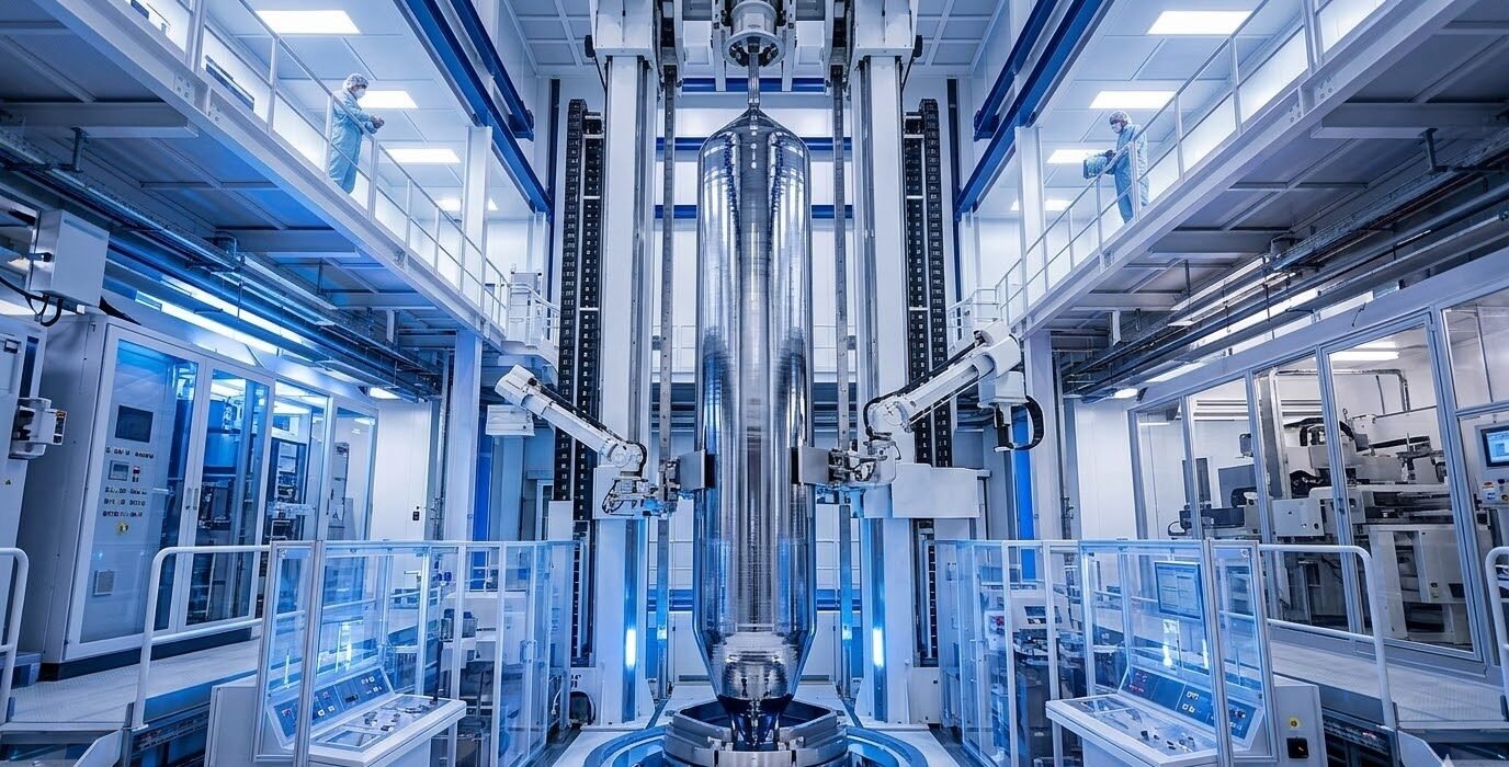
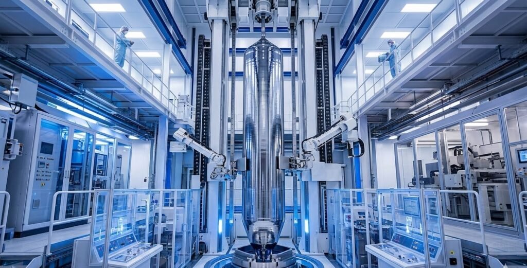
The pursuit of efficiency and cost reduction in high-tech industries often hinges on the ability to scale. In the world of advanced materials, this translates to the challenge of large-diameter crystal growth. Producing larger industrial crystals, whether silicon for semiconductors or halides for radiation detection, offers significant economies of scale but introduces formidable technical hurdles.
Thermal Stress and Defect Management
As the diameter of a single crystal increases, controlling the thermal environment becomes exponentially more complex. Thermal stress management is perhaps the most critical challenge. Large crystal ingots develop significant temperature gradients during growth and cooling. If not meticulously controlled, these gradients can induce severe thermal stress, leading to dislocations, cracking, and a marked reduction in crystal quality. The entire single crystal technology must adapt, requiring advanced insulation, sophisticated multi-zone heating systems, and incredibly precise temperature ramp-down protocols to mitigate these risks.
Melt Stability and Hydrodynamics
The dynamics of the molten pool also change dramatically with size. Maintaining melt stability control becomes far more difficult as the volume increases. In a larger crucible, complex convective flows and turbulent patterns can emerge, destabilizing the growth interface. This can cause fluctuations in the crystal diameter and non-uniform doping—a critical failure in semiconductor silicon. Innovations in magnetohydrodynamics (MHD) and advanced process modeling are increasingly employed in modern advanced crystal growth systems to simulate and stabilize these large-volume melts.
The Path Forward: Integration and Automation
Successfully scaling crystal production requires a holistic approach, integrating materials science, mechanical engineering, and advanced control theory. The future of the industry lies in increasingly automated, adaptive growth systems capable of real-time monitoring and process correction. Only by overcoming these fundamental engineering challenges can we fully unlock the potential of large-diameter industrial single crystals.